Pin Description:
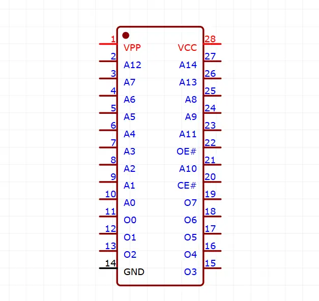
| Pin No | Pin Name | Description |
| 1 | 1G’ | Channel 1 output enable |
| 2 | 1A1 | Channel 1, (A) side 1 |
| 3 | 2Y4 | Channel 2, Y side 4 |
| 4 | 1A2 | Channel 1, (A) side 2 |
| 5 | 2Y3 | Channel 2, Y side 3 |
| 6 | 1A3 | Channel 1, (A) side 3 |
| 7 | 2Y2 | Channel 2, Y side 2 |
| 8 | 1A4 | Channel 1, (A) side 4 |
| 9 | 2Y1 | Channel 2, Y side 1 |
| 10 | GND | Ground |
| 11 | 2A1 | Channel 2, (A) side 1 |
| 12 | 1Y4 | Channel 1, Y side 4 |
| 13 | 2A2 | Channel 2, (A) side 2 |
| 14 | 1Y3 | Channel 1, Y side 3 |
| 15 | 2A3 | Channel 2, (A) side 3 |
| 16 | 1Y2 | Channel 1, Y side 2 |
| 17 | 2A4 | Channel 2, (A) side 4 |
| 18 | 1Y1 | Channel 1, Y side 1 |
| 19 | 2G’ | Channel 2 output enable |
| 20 | VCC | Positive Supply |
Specifications:
| Parameter | Condition | Min | Typ | Max | Unit |
| Supply Voltage (Vcc): | 4.75 | 5 | 5.25 | V | |
| High-Level Input Voltage: | 2 | V | |||
| Low-Level Input Voltage: | 0.8 | V | |||
| Propagation Delay: | 12 | 18 | ns | ||
| Output Current (Low): | 24 | mA | |||
| Operating Temperature: | 0 | 70 | °C |
Footprint Diagram:

Applications:
- Memory Address Driving.
- Clock Driver.
- Bus Transceiver.
- System Bus Buffering.
- General Purpose Line Driving.
Products related to this item
These other products might interest you
See also
Your Dynamic Snippet will be displayed here... This message is displayed because you did not provide both a filter and a template to use.
Last featured
Check out if you want this too !
Your Dynamic Snippet will be displayed here... This message is displayed because you did not provide both a filter and a template to use.


