74138 IC High Speed 1 Line of 8 Line Decoder/ Demultiplexer DIP-16
The 74138 (SN74LS138 / LS138 family) is a low-power Schottky (LS) 1-of-8 decoder / Demultiplexer that accepts three binary-weighted inputs (A0, A1, A2) and, when enabled, activates one of eight mutually exclusive active-LOW outputs (O0–O7). Two active-LOW enables and one active-HIGH enable simplify cascading and expansion, letting multiple devices be combined to form larger decoders.
When the proper enable combination is present (E1 and E2 LOW, E3 HIGH), the device decodes the three address inputs and drives exactly one output LOW while the others remain HIGH. Inputs are fully buffered and include Schottky clamp diodes to reduce ringing and improve high-speed switching integrity in bipolar memory and data-routing systems.
The LS138 is designed for TTL logic-level systems (VCC ≈ 5 V) and is commonly used where a compact, fast address decode or demultiplexing function is required. The device is available in multiple package types (PDIP, SOIC, SOP, etc.) and temperature/qualification variants.
Features:
- High-speed 1-of-8 decoding / demultiplexing.
- Schottky-clamped inputs for improved switching and reduced ringing.
- Three enable inputs (two active-LOW, one active-HIGH) for easy cascading and expansion.
- Fully buffered inputs (single normalized load to driving circuit).
- Mutually exclusive active-LOW outputs.
- Available in PDIP, SOIC, SOP and other package variants.

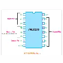
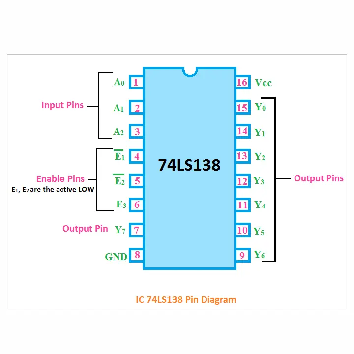
74LS138 Pin configuration:
74LS138 is a sixteen-pin device as shown in the pin diagram and we will describe the function of each pin below.
| Pin | Name | Description |
| 1 | A | Address input pin |
| 2 | B | Address input pin |
| 3 | C | Address input pin |
| 4 | G2A | Enable input (active LOW) |
| 5 | G2B | Enable input (active LOW) |
| 6 | G1 | Enable input (active HIGH) |
| 7 | Y7 | Output pin 7 |
| 8 | GND | Ground |
| 9 | Y6 | Output pin 6 |
| 10 | Y5 | Output pin 5 |
| 11 | Y4 | Output pin 4 |
| 12 | Y3 | Output pin 3 |
| 13 | Y2 | Output pin 2 |
| 14 | Y1 | Output pin 1 |
| 15 | Y0 | Output pin 0 |
| 16 | VCC | Power supply pin |
Specifications:
| Physical | |
| Case/Package: | PDIP |
| Contact Plating: | Gold |
| Mount: | Through Hole |
| Number of Pins: | 16 |
| Technical | |
| Bandwidth: | 35 MHz |
| High-Level Output Current: | -400 µA |
| Independent Circuits: | 1 |
| Input Current: | 100 µA |
| Logic Function: | Decoder, Demultiplexer |
| Low-Level Output Current: | 8 mA |
| Max Operating Temperature: | 70 °C |
| Max Power Dissipation: | 1 mW |
| Max Supply Voltage: | 5.25 V |
| Min Operating Temperature: | 0 °C |
| Min Supply Voltage: | 4.75 V |
| Number of Bits: | 8 |
| Number of Channels: | 1 |
| Number of Circuits: | 1 |
| Number of Elements: | 1 |
| Number of Input Lines: | 3 |
| Number of Inputs: | 3 |
| Number of Output Lines: | 8 |
| Number of Outputs: | 8 |
| Operating Supply Voltage: | 5 V |
| Polarity: | Inverting |
| Propagation Delay: | 41 ns |
| Quiescent Current: | 6.3 mA |
| Supply Type: | Single |
| Turn-On Delay Time: | 41 ns |

Applications:
- Line decoders
- Servers
- Digital systems
- Line De-multiplexing
- Telecom circuits
- Memory circuits
Products related to this item
These other products might interest you
See also
Last featured
Check out if you want this too !